Generate FIFO Interface DPI Component for UART Receiver
此示例显示了如何生成用于与UART接收器集成的FIFO缓冲区接口的SystemVerilog DPI组件的完整工作流程。该界面用MATLAB编写,并导出到HDL模拟器。还提供了UART接收器及其测试工作台的SystemVerilog文件。
For demonstrative purposes, this example uses Modelsim 10.3c in 64-bit Windows 7. However, this same procedure can be easily replicated for other systems and simulators.
Requirements and Prerequisites
Products required for this example:
MATLABCODER®
Simulators: Mentor Graphics® ModelSim®/QuestaSim® or Cadence® Incisive
One of the supported C compiler: Microsoft® Visual C++, or GNU GCC
Background
通用异步接收器和发射器(UART)是通过串行线发送和接收数据的电路。UART通常与RS-232标准一起使用,并包含接收器和发射器。但是,在此示例中,仅使用一个接收器。
The serial transmission starts with a 'start bit' which is 0, followed by data bits, and ends with a 'parity bit' and a 'stop bit'. Transmission of a single byte is show in the following figure:
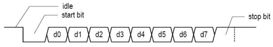
The transfer is asynchronous, which mean that there is no clock information, therefore the receiver and transmitter must agree on what baud rate,stop bits and parity bit are used. In this example one byte will be transferred with a baud rate of 19,200, 1 stop bit and no parity bits.
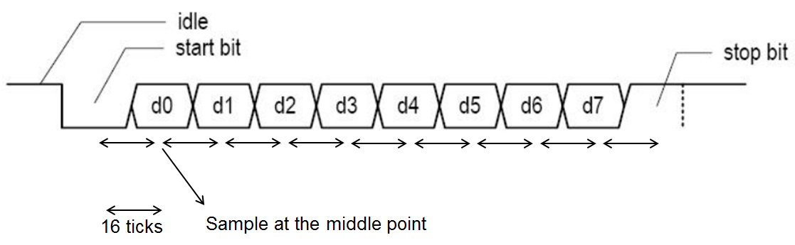
An oversampling scheme will be used to estimate the middle point of the data bit at a rate 16 times the baud rate, as shown in the figure below.
The following schematic illustrates the UART receiver design.

Step 1: MATLAB Design
第一步是编写满足设计要求的MATLAB代码,您应该尝试在测试台中捕获要求。在此示例中,我们的设计包括8个单词的第一个(FIFO)缓冲区。
Design:FIFO_Buffer
Test Bench:FIFO_BUFFER_TB
Step 2: Make sure the MATLAB testbench captures the requirements
运行测试台以确保没有运行时错误,以下图应绘制。
FIFO_BUFFER_TB

请注意,TestBench正在以以下方式行使设计:
Clock cycles<15: Write 6 bytes (write signal enabled, read signal disabled), then Read the 6 bytes (read signal enabled,write signal disabled).
Clock cycles>15: Read and write simultaneously.(For example: The byte that is written is read in the next clock cycle).
Step 3: Generate the DPI component and verify the behavior in the HDL Simulator
要生成组件执行以下命令:
dpigen-试验台FIFO_BUFFER_TBFIFO_Buffer-args{0,int8(0),0}
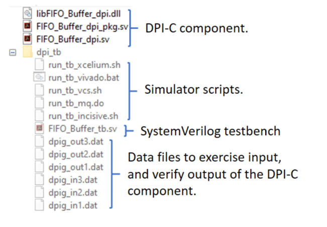
下图显示了此示例的相关文件。
Once DPIGEN generates the DPI component and its testbench you can run the SystemVerilog testbench by following the steps below:
在GUI模式下启动ModelsIm/QuestAsim。
Change your current directory to "dpi_tb" under the code generation directory in your HDL simulator.
Enter the following command to start your simulation
dorun_tb_mq.do
将生成以下波形形式:
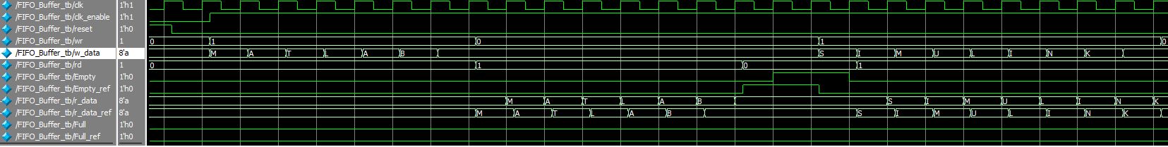
Note that this matches our MATLAB testbench where we write 6 bytes and then read them,followed by simultaneously writing and reading 8 bytes.
When the simulation finishes, you should see the following text printed in your console:
**************TEST COMPLETED (PASSED)**************
步骤4:将生成的DPI组件集成到UART接收器设计中
After the DPI component behavior has been verified, it is time to integrate it into the UART receiver. The following figure shows the files required for the different components.
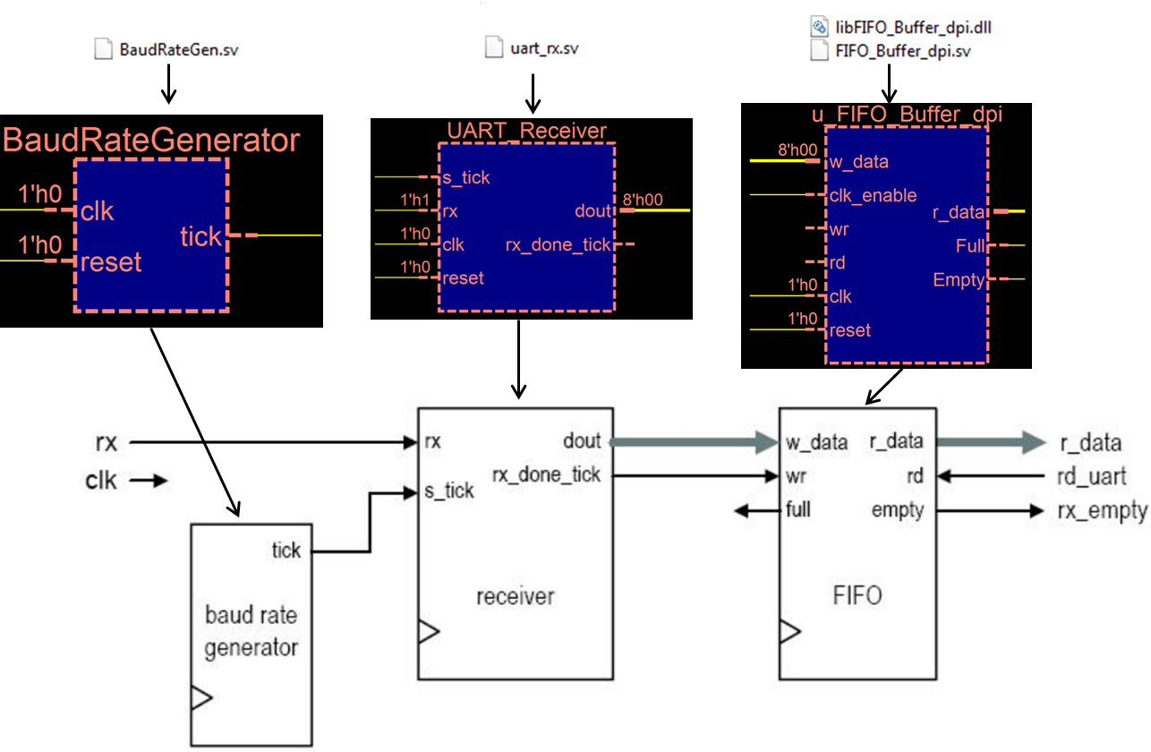
To exercise the UART receiver with the DPI component integrated, the testbench named 'uart_rx_FIFO_tb.sv' has been provided. To integrate the component all that is needed is to instantiate the component in the testbench as shown below:
// Instantiate DUT generated using MATLAB Based SystemVerilog DPI FIFO_Buffer_dpi u_FIFO_Buffer_dpi( .clk(clk), .clk_enable(clk_enable), .reset(reset), .wr(rx_done_tick), .w_data(dout), .rd(rd), .Empty(Empty), .r_data(r_data), .Full(Full) );
步骤5:模拟UART接收器
要成功模拟设计,请确保以下文件在同一文件夹中:

类似于第三步,打开Modelsim并运行,file using:
dorun_tb.do
The following wave forms are generated:

在TestBench中,6个ASCII字母('Matlab')通过串行“ RX”信号传输,并写入FIFO缓冲区。在第六个字母传输完成后,主张“ RD”信号将“ r_data”中的字母(“ matlab'”)恢复。
参考
Pong P. Chu (2008), FPGA Prototyping by Verilog Examples. Hoboken, New Jersey: John Wiley & Sons, Inc.
选择一个网站
Choose a web site to get translated content where available and see local events and offers. Based on your location, we recommend that you select:.
Selectweb site您还可以从以下列表中选择一个网站:
Americas
- AméricaLatina(Español)
- Canada(English)
- United States(English)
欧洲
- Belgium(English)
- 丹麦(English)
- Deutschland(德意志)
- España(Español)
- Finland(English)
- 法国(Français)
- 爱尔兰(English)
- 意大利(Italiano)
- Luxembourg(English)
- Netherlands(English)
- 挪威(English)
- Österreich(德意志)
- Portugal(English)
- Sweden(English)
- 瑞士
- 英国(English)