如果接收器系统的架构设计
此示例显示如何使用RF Blockset™电路包络库模拟具有以下RF损伤的架构的低电平的性能:
组件噪声
阻塞信号的干扰
LO相位噪声
模数转换器(ADC)动态范围
组件不匹配
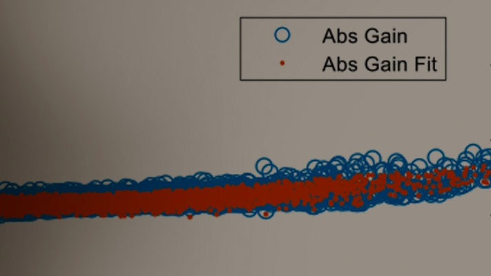
Design variables in the RF portion of the model include explicit specification of gain, noise figure, IP3, input/output impedance, LO phase offset, and LO phase noise. Carrier frequencies for waveforms entering RF Blockset subsystems are specified in the Inport blocks. Design variables for the transmitter side of the RF interface include carrier frequency, modulation scheme, signal power, and blocker power level. Baseband design variables are number of bits and full scale range of the ADC.

系统架构:
该模型说明了ISM频带接收器的设计和仿真。主子系统包括数字发射器,RF接收器,ADC,用于噪声LO建模的相位噪声块和数字接收器。其余块用于分析。


The digital transmitter consists of three FSK modulated waveforms and a high power tone. The three FSK waveform generators use a bandlimiting filter that suppresses the FSK sidebands below the expected thermal noise level. The target waveform at 2450 MHz has a 1 ohm referenced passband power level of approximately -70 dBm. Similarly defined image and intermodulation distortion (IMD) blocker waveforms have passband powers of approximately -40 dBm and -33 dBm, respectively. The IMD tone that couples with the IMD blocker to generate in-band IM3 products has a passband power of -33 dBm. Since the baseband processing defines the complex envelope waveforms, computing passband power requires the insertion of 1/sqrt(2) gain as shown in the design. An IF of 2 MHz can be inferred by inspecting the demodulator input signal spectrum, where a 2 MHz offset is specified for the display.

如果接收器的低,则由接收带SAW滤波器,频率转换级,图像抑制阶段和两个增益级组成。电阻用于模拟输入和输出阻抗。每个非线性块具有噪声数字规范。低噪声放大器(LNA)中的电源非线性,如果放大器和混频器由IP3指定。通过Hartley设计完成图像抑制,单个LO和相移块可以分别提供与I和Q分支混合的余弦和正弦术语。求和块重新组合I分支和相移Q分支上的信号。通过在相移块中设置非理想相位偏移可以直接控制图像抑制质量。要捕获RF,图像,IMD信号和IMD音频波形/光谱,请选择基本的音调to be 2450 MHz, 1 MHz and the谐波作为第一个音调和8个用于配置块的第二音的1。在RF块集环境中模拟热噪声底板,Temperature在配置块中的系统参数部分内设置为290.0 K的噪声温度。

ADC使用12位量化器进行建模。量化器考虑了ADC的全尺度和动态范围,适当地建模其量化噪声底板。
数字接收器解调有关误码率计算的波形。该非组织FSK接收器假设完美的时序同步,使得每个FSK脉冲集成在一个且仅一个符号上。
运行该示例
运行该示例模拟了一个符合未编码的BER规范的设计,低于1%。对接收器和ADC中的信号和组件规范的修改对接收器性能直接影响。手动交换机使您可以:
为IMD阻止器音的功率电平-33 dbm或-45 dBm选择电量
选择理想或嘈杂的LO。
Other possible changes to the design include:
Image rejection ratio (IRR) of the Hartley design. The IRR of the present design (dPhi=0.01 degrees) is -40 dB. For more information on calculating IRR, see the example
测量接收器中的图像抑制比测量接收器中的图像抑制比>。
调制方案
Baseband filtering options
信号功率水平
信号载波频率
噪音数字
Non-linear gain parameters
级间匹配ing
ADC位长度和满量程范围