使用行为和EM仿真,带有开放微带线存根的带式和带通滤波器
This example shows different ways to create microstrip Line Bandpass and Bandstop filters using open circuit stub.
Thepcbelement.object is used to convert the RF PCB catalog into a circuit element and a Tee shaped circuit is built. The circuit is analysed using the behavioral model and EM simulation. The traceTee shape in RF PCB Toolbox is used and converted into a PCB component and analysed. The PCB is analysed using EM Simulation and the results are compared with the circuit counterpart.
The dimensions of the microstrip line and the stub in the figure are taken from the reference. The left image shows the circuit representation with the port numbers and the right side image shows the traceTee structure with same dimensions.


Circuit Element with Behavioral Model for Microstrip Line
创建一个circuitobject and three微带素用于构建电路的对象,如图所示。将EPSILONR和高度的值更新为2.33和1.57 mm。
tic ckt = circuit; c1 = microstripLine('长度',46e-3,'Width',4.6e-3);c1.Substrate.EpsilonR = 2.33; c1.Height = 1.57e-3; c2 = microstripLine('长度',46e-3,'Width',4.6e-3);c2.substrate.epsilonr = 2.33;c2.height = 1.57e-3;C3 =微带素('长度',18.4e-3,'Width',4.6e-3);c3.Substrate.EpsilonR = 2.33; c3.Height = 1.57e-3;
Use thepcbelement.对象将微带线转换为电路对象并设置行为的flag to真的因此,计算将使用分析方程式完成。在电路模型中,没有建模微带不连续性,因此结果可能与EM分析略有不同。
p = pcbElement(c1,'Behavioral',真的);p1 = pcbElement(c2,'Behavioral',真的);p2 = pcbelement(c3,'Behavioral',真的);
Use the add function to form the circuit and use the ports numbers as shown in the circuit above. Use port numbers 1 and 2 for the first microstrip line and connect another microstrip line from ports 2 to 3 which forms a series connection. Connect the third microstrip line from the port 2 to 4 which forms a tee network.
添加(ckt,[1 2 0 0],p);添加(CKT,[2 3 0 0],P1);添加(CKT,[2 4 0 0],P2);setports(ckt,[1 0],[3 0]);
Use thesparameters函数来计算电路的S参数并使用该方法绘制它rfplot功能。
S = sparameters(ckt,linspace(1e9,10e9,21)); figure,rfplot(S);
Circuit Element with EM simulation for Microstrip Line
Use thepcbelement.对象将微带线转换为电路对象并设置行为的flag tofalse因此,计算将使用EM仿真完成。
ckt1 = circuit; p = pcbElement(c1,'Behavioral',错误的);p1 = pcbElement(c2,'Behavioral',错误的);p2 = pcbelement(c3,'Behavioral',错误的);
Use the add function to form the circuit and use the ports numbers as shown in the circuit above. Use port numbers 1 and 2 for the first microstrip line and connect another microstrip line from ports 2 to 3 which forms a series connection. Connect the third microstrip line from the port 2 to 4 which forms a tee network.
add(ckt1,[1 2 0 0],p); add(ckt1,[2 3 0 0],p1); add(ckt1,[2 4 0 0],p2); setports(ckt1,[1 0],[3 0]);
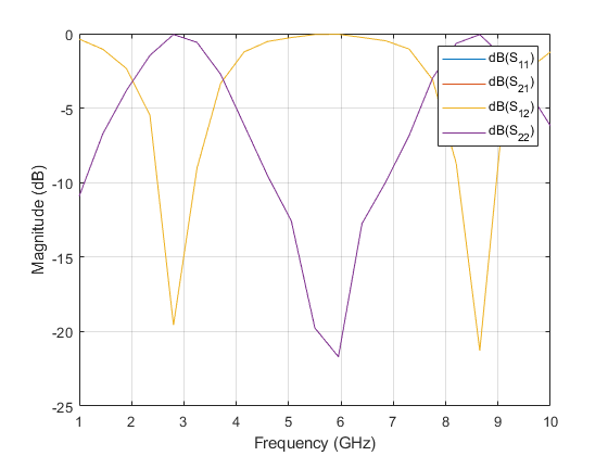
Use thesparameters函数来计算电路的S参数并使用该方法绘制它rfplot功能。使用EM求解器求解每个微带部分,并将计算的S参数组合以提供电路的组合响应。
S = sparameters(ckt1,linspace(1e9,10e9,21)); figure; rfplot(S);

Creating PCB Stack of traceTee Shape with EM Simulation
Use thetraceTeeshape to create the open circuit stub and use the dimensions as shown in the figure above and visualize it.
obj = traceTee; obj.Length = [92e-3 18.4e-3]; obj.Width = [4.6e-3 4.6e-3]; figure; show(obj);

Use thepcbComponentto convert the shape into a PCB stack. ThepcbComponentcreates the PCB stack up for traceTee shape and assigns the FeedLocations at the three open ends of the shape. Assign the dielectric and groundplane to theLayers财产的财产pcbComponent. Also assign theBoardShapeto the grounplane. In the current design, the stub is required as open circuit, hence delete the feed at the third location.
pcb = pcbComponent(obj); gnd = traceRectangular('长度',92e-3,'Width',90e-3); d = dielectric('EpsilonR',2.33);pcb.boardthickness = 1.57e-3;pcb.layers {2} = D;PCB.Layers {3} = GND;pcb.boardshape = gnd;PCB.FeedLocations(3,:) = [];数字;展示(PCB);

Use the网function to manually mesh the structure and set theMaxEdgeLengthto 10 mm.
图,网格(PCB,'MaxEdgeLength',10e-3);

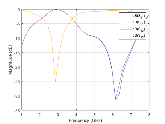
Use thesparametersfunction to calculate the s-parameters of the structure and plot it usingrfplot功能。
S1 =散差(PCB,Linspace(1E9,8e9,35));数字;RFPLOT(S1);
Design at Specific Frequency
BandStop滤波器的谐振取决于需要在谐振频率处的四分之一波长的短线长度。在上面的示例中,短截线是四分之一波长在2.9 GHz下,因此在该频率下观察到谐振。如果在任何其他频率下预期谐振,则需要在该频率处的四分之一波长。
参考
Alexander B. Yakovlev, Ahmed I. Khalil , Efficient MOM-based generalized scattering matrix method for the integrated circuit and multilayered structures in waveguide
选择网站
Choose a web site to get translated content where available and see local events and offers. Based on your location, we recommend that you select:.
Selectweb site您还可以从以下列表中选择一个网站:
Americas
- América拉丁(español)
- Canada(English)
- United States(English)
欧洲
- Belgium(English)
- 丹麦(English)
- Deutschland(德意志)
- España(español)
- Finland(English)
- 法国(Français)
- 爱尔兰(English)
- 意大利(Italiano)
- Luxembourg(English)
- Netherlands(English)
- 挪威(English)
- Österreich(德意志)
- Portugal(English)
- Sweden(English)
- 瑞士
- 英国(English)